Animated Functional Diagram F21
F21 Microprocessor Prototype Chips C,D
Animated Functional Diagram F21
F21d went into Mosis on 8/28/98. The chips should be returned from Mosis for packaging around the end of November 98.
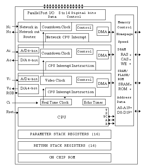
The F21 microprocessor contains a Stack Machine CPU, a video i/o coprocessor, an analog i/o coprocessor, a serial network i/o coprocessor, an parallel port, a real time clock, some on chip ROM (*not on F21d), and an external memory interface.
PDF F21d pinout and
Preliminary PDF Data Sheets for F21 were posted
on 9/13/98
F21 is being fabricated .8 micron CMOS technology using the HP process at Mosis. F21 is being prototyped in a 68 pin ceramic package similar to the 68 pin PLCC that will be used for production. Click here to see the An F21 simulator and an F21 emulator are available in the Ultra Technology Online Store.
It will access to 3 memory spaces, one megaword of 20 bit wide DRAM, 8K words of 20 bit wide fast SRAM, and one megabyte of 8 bit wide PROM, SRAM, FRAM, or PCMCIA CARD memory for booting. It will interface directly to 5 1Mx4 or 265Kx4 DRAMS and/or 3 8Kx8 high speed SRAM. A system can be built with only 5 or 7 chips. Memory timing for the three memory spaces are: 150ns or 250ns for 8 bit SRAM, 40ns onpage and 140ns offpage 20 bit DRAM, and 12ns or 25ns for 20 bit fast SRAM. All memory timings are adjustable within a +20% to -40% speedup range. The interal ROM has an 8ns setup and 4ns load time for a total access time of 12ns. The chip also provides a parallel I/O port decoded and latched on chip.
The memory interface processor provides memory access to all processors giving lowest priority to the CPU. The I/O coprocessors can be turned on or off by the CPU, and can run continuously executing their own instructions, or can interrupt the CPU to process their data buffers or instructions.
F21b had 3 power and 3 ground pins as did early i21 chips. F21d has 6 power and 6 ground pins. This may be more than needed and a production part or less and some of the port pins may become power and ground pins or visa versa.
As with F21c F21d will not have composite video out or video input functionality. On F21c there are no Vo and Vi pins. The video coprocessor on this prototype has RGB output only. Composite 3 level grey is available on the G pin in programmable resolution.
There have also been changes to the parallel port on F21c. The extra SRAM addressing lines and serial/network pins are also mapped to parallel port lines so that they can be used as parallel port i/o bits if they not being used for SRAM addressing or serial networking. It will also permit the Serial Out line to be tri-stated to support multiple network topologies.
There is also one more SRAM addressing bit A13 on P13. This allows for direct addressing of 16K words of high speed 20 bit wide SRAM to take full advantage of the 16K word sized Home Page addressing feature.
![]()
2512 10th Street
Berkeley, CA 94710