Page under construction 1/26/01
F21 Analog I/O Coprocessor
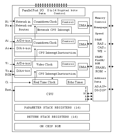
Theory of Operation
External Circuitry
Internal Design
Operation
Testing
Analog Instruction/Data Word Format
F21 Control Registers
Analog Control Register Format
Software
Theory of Operation
The Analog Coprocessor on F21 is a simple and fast device for reading and/or writing Analog samples on the F21 Ai and Ao pins. The sample rate of the F21 Analog Coprocessor is controled by the external clock oscilator signal and an internal count down control register. On each external clock this eleven bit register is counted down. Whenever it reaches zero the Coprocessor clocks Analog sampling and resets the count down register from 11-bits in the Analog I/O Coprocessor control register, Ca. The 11-bit count down value is set with a pattern (F21 number xored with AAAAA) with a value from 1 to 2047. The Analog sample rate, As, is thus As = CLK/counter.
If analog countdown = 1 then As = CLK. If Analog countdown = 2 047 then As = CLK/2047. A production F21 may have separate input clocks for Analog, video and network. F21d uses one input clock, CLK, for all three I/O Coprocessors. The video coprocess has no count down register and runs at CLK, thus if F21d is generating video CLK will be from 7.2 Mhz (384x482 NTSC) to 25.75 Mhz (VGA) and Analog sample rates will be from those high values down to 3.6 Khz to 12.87 Khz. Fast SRAM is used exclusively for the Analog I/O Coprocessor to get the maximum Analog throughput with F21d.
F21d
256 values from 0 to 2.5 V
40 Msps maximum sample rate
External Circuitry
One can connect the F21 Analog pins directly to devices in some applications. In this mode the individual samples each have eight bits of resolution. For applications requiring higher output precision one can use oversampling and property of the output devive to integrate the signal. This trades sample rate for precision. With two times oversampling a bit can be 0,0 0,1 1,0 or 1,1. The integration of the attached device will get values halfway between the lowest bit of precision this way.
One can also connect F21 to inexpensive operational amplifiers operating as differential amplifiers. This is another technique to trade sample rate for precision. The fixed values from the F21 D/A are converted to relative values by the differential circuit. At four times oversampling four analog samples are combined to provide four times the range, two extra bits of analog resolution.
One can provide more elaborate external circuitry using a combination of analog input, analog out, and digital input and outputs for more complex interfaces.
Internal Design
F21d is constructed in .8u process CMOS technology. The process manuals conservatively state that the process is fast enough to support a 75 Mhz flip-flop. The internal circuits in F21d are far more highly tuned. Internally F21d has one 10 Gigahertz Digital to Analog converter connected to the analog output pin and another connected to a Schmitt trigger threshold detector. The input is sampled by isolating the voltage on a capacitor. This voltage is slowly increased until it reaches a Schmitt trigger threshold. The time this takes is counted. So the count measures the difference between input and ~3 V. After calibration, a table lookup with the count will give the voltage. Smaller counts imply higher voltage.
The F21d Analog Coprocessor has 8 bit input and output circuits. The D/A outputs a value. When the value of the Analog input signal is determined it is latched and available to be written back to memory in the low 8 bits of the word.
In each clocked Analog sample the Analog I/O Coprocessor:
reads a location in memory with an Analog I/O Coprocessor instruction/data word,
reads the bits to be output through a flash D/A to the Analog output pin, Ao.
samples and holds the value on the Analog input pin, Ai,
does an A/D conversion with up to 256 step comparisons,
inserts the converted digital value of Ai into the low
bits of the value read from memory,
writes it back to memory,
resets the count down Analog timing register,
increments the bottom ten bits of the Analog instruction/data pointer,
and if the interupt instruction bit is set it sets the analog flag bit in the memory control register,
and forces a CPU interupt in place of the next CPU instruction load.
The CPU interupt will push the current value of the CPU program counter to the return stack, and jump to address zero on the current homepage to begin executing an interupt service routine. If there is more than one interupt in operation the routine must determine the interupt source and clear the designation bit. Analog input buffers can then be read by the CPU and analog output buffers can be written.
All of the analog processing by the Analog I/O Coprocessor requires only one memory write-after-read cycle on the bus. Normally only one CPU interupt needed for every 1000, or 1024 samples. This type of operation is quite different than designs that require a CPU interupt on every sample since this requires many more memory operations per sample. A CPU interupt can occur with each analog sample if the programmer chooses by setting the CPU interupt instruction bit in each analog instruction provided the sample rate is low enough to provide sufficient memory bandwidth.
Since the Analog input ramp encoder circuit must make 256 steps to convert a sample from Analog to digital 10G/256 gives a 40 Msps (Mega sample per second). This matches giving the full memory bandwidth of F21d with fast SRAM memory to Analog I/O Coprocessor. In practice memory bandwidth must be balanced between I/O Coprocessors and the CPU so it will determine the maximum Analog sample rate.
Operation
On each Analog sample a data word is read, then written back to DRAM. Bits 19-12 are sent to a binary 8-bit D-A converter. The memory word is re-written with bits 7-0 from an 8-bit A-D converter. Current output is 0 - 100 mA over a range of 0 - 2.5 V.
The Analog I/O Coprocessor is first pointed to an address in memory and then started. It will not change the upper 11 bits of the address and will remain on the same 10 bit page of memory. It will not increment its address beyond that 10 bit page. That is, 0FFFFF increments to 0FFC00. Thus Analog output cycles within a DRAM page if no CPU interupts are invoked. If no CPU interupts are invoked the Analog I/O Coprocessor will repeatedly record and play 1K word worth of samples.
If bit 10 is set in the Analog I/O Coprocessor instruction/data word the CPU is interrupted. At the next CPU instruction fetch a call to 0000 on homepage will be inserted. The interrupt is automatically cleared. In normal operation an interupt instruction is set at or near the end of the 1K block of Analog instruction/data words. When invoked the Analog I/O Coprocessor CPU interupt instruction will direct the CPU to service the Coprocessor. In the case of data output the next 1K of output data will be moved by the CPU into the memory being used by the Analog processor. For data input the CPU will copy the old data and perhaps do some further processing such as DSP routines on the sampled data.
The Analog I/O Coprocessor control register uses 13 bits, 11 for the count down timing register and 2 other control bits. In Ca Bit 18 is the on/off control bit. When set the Analog I/O Coprocessor runs. In Ca bit 1 specifies that the CPU is about to transfer the address of the Analog I/O Coprocessor instruction/data buffer. If bit 1 is set, the next address the CPU provides will be incremented and latched into the Analog I/O Coprocessor instruction address register. The opcode that writes to the Ca register must be in the same instruction word as the opcode that reads or writes the address that is to be transfered from the CPU to the coprocessor. If they were not in the same word the coprocessor would latch the address of the next CPU instruction as it would be the next value on the bus.
Testing
For initial testing no video will be generated and a slow 1.8 Mhz clock oscilator will be used. This will provide a sample rate from 1.8 Mhz to 0.9 Khz. Continuous (looping) Analog output with no interupt will be the first test. Precision and linearity will be measured. Analog input will then be tested followed by analog interupt. Finally the count down register and speed range of the processor will be checked.
Analog Instruction/Data Word Format
Analog I/O Coprocessor instruction/data word format (as pattern):
data:  input i0-i7 = d0-d7,
       output o0-o7 = d12-d19
instruction: d10 = CPU interupt
bit #
19, 18, 17, 16, 15, 14, 13, 12, 11, 10,  9,  8,  7,  6,  5,  4,  3,  2,  1,  0
o7  o6  o5  o4  o3  o2  o1  o0   0  int  0   0  i7  i6  i5  i4  i3  i2  i1  i0
F21 Control Registers
pattern number
1C0007  16AAAD Cm Configuration memory, write to clear 3 int flags
                  DRAM timing, SRAM timing, ROM timing, overall timing, homepage,
                  ROM page, RAS after CAS, 9 bit page, clear int flags
1C0001  16AAAB Cm Configuration memory, write to clear int flag 1 (analog?)
1C0002  16AAA8 Cm Configuration memory, write to clear int flag 2 (video?)
1C0004  16AAAE Cm Configuration memory, write to clear int flag 4 (serial?)

1C0240  16A8EA Cv Configuration video
                  video on/off, pass address


1C0600  16ACAA Ca Configuration analog (original doc)
                  analog on/off, analog rate, pass address (correcte0d 1/26/01)

1Cxxxx  16xxxx Cn Configuration serial network
                  forward input, on/off, serial rate, word/byte, pass address, xmit
1Cxxxx  16xxxx Cs Configuration Start of message token (SOM)
1Cxxxx  16xxxx Ce Configuration End of message token (EOM)

1C2200  1688AA Rc Realtime Clock
                  real time clock, ext clock or video int input
                  (1000p ! is video int inc real time clock)

1C0300  16A9AA P  Parallel Port I/O data (inverted pattern)
1C0280  16A82A Pd Parallel Port direction
                  direction, bias, serial handshake, serial bits, serial tristate, SRAM adr
Analog Control Register Format
Analog I/O Coprocessor control register, Ca: (13 control bits)

Analog I/O Coprocessor control register format (as pattern):
bit # function
18    on/off (0 at reset)
6-16  rate - count down register reset bits
1     pass address from CPU

bit #
19, 18, 17, 16, 15, 14, 13, 12, 11, 10,  9,  8,  7,  6,  5,  4,  3,  2,  1,  0
 x  on   x  r10 r9  r8  r7  r6  r5  r4  r3  r2  r1  r0   x   x   x   x  adr  x
    on/off  ----------- count down rate --------------             transfer/adr
Odd bits are inverted in pattern/number conversion (AAAAA xor) so when
viewing Ca as a number,
bit 1 off signifies a transfer of the Analog buffer address from the cpu, and
bit 18 on signifies Analog processing turned on (since it is an even bit).In the original doc Chuck said, "Ca is to be loaded with a value for a 11-bit pseudo-random shift register (Ca.0 = Ca.10 -or Ca.8)" I am not sure what he meant by that. I assume I just insert an 11 bit number and convert to a pattern...
With the addition of two more control bits in the Analog control regitser, Ca, or in the Analog Coprocessor instruction set, F21 could specify input, output, or Analog input after Analog output, the default operation in F21d.
Software
\ Some examples of Analog Control register values:
\
\ pattern number  function
\ 00040p AAAEA# = analog off, count=1
\ 40040p EAAEA# = analog on, count=1
\ 40080p EAA2A# = analog on, count=2
\ 40042p EAAE8# = analog on, count=1, transfer buffer address
\ 1FFC0p B556A# = analog off, count=2047
\
\ to start analog I/O
\
                  \ Ca = 1C0600p 16ACAA# = 95355 # com (1/26/01)
 A 95355 # com A! \ save A, place address of Analog Control register in A
 01000 # nop      \ address of the Analog buffer to be transfered in N
 EAAE8 # nop      \ analog on, count=1, transfer buffer address
 !A A! @A drop    \ @A must be in same word as !A
                  \ turn on analog, set count down reg, transfer next addr
                  \ set A to the Analog buffer and do a read to transfer it
                  \ to the to Analog I/O coprocessor instruction pointer
 A! nop nop nop   \ restore the A register
If there are any interupt instructions in the Analog I/O Coprocessor
instruction/data words when Analog processing is running then
an interupt service routine is needed at 0000 on the current homepage.The mininal interupt service routine is ; (subroutine return)
There are three bits in the memory control register that show the source of interupts. The low 3 address bits control which interupt source flag bits will be cleared in the memory control register.
\ It is intended that this code be executed
\ at the end of an Analog I/O Coprocessor interrupt service routine:

 A 95554 # com A! \ 1C0001p 16AAAB# Cm to clear int bit 1, analog flag
 @A !A A! ;       \ clear int bit, restore A, return
![]()
Page under construction 1/26/01
![]()
Document updated 1/26/01