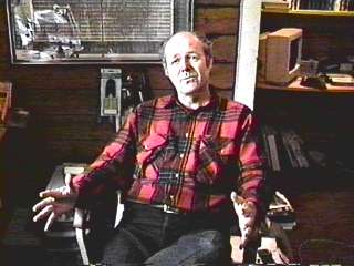
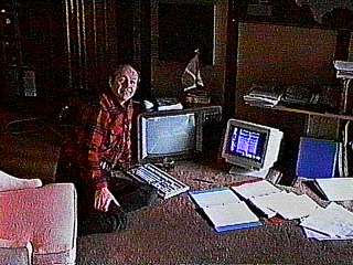
![]() Chuck Moore interviewed in his home office on 6/6/93.
A
video of this presentation in the store.
Chuck Moore interviewed in his home office on 6/6/93.
A
video of this presentation in the store.
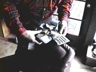
On 6/6/1993 Chuck Moore gave the following interview from his home. He began with a tour of the "museum", the very first Forth hardware board.
Chuck: Here behind glass, in fact behind glasses, I have one of the early, early computers. I very rarely get this out so it is a good excuse to see what is left up here. Here is one of the naked die of a P21 and here is a pile of wires and boards which I think is the earliest NOVIX computer. These are a number of interface boards all cabled together with the basic I guess one of the early Forth kit boards. There is the NOVIX and all of its static RAM. These boards collectively generated video.
I know that because that is all I did with these interface boards is generate
video. Again this is one of the reasons for putting a video coprocessor
on the P21. If you don't plan ahead you can get into a real mess trying to
work things up afterwards. Incidentally that is what happened on the PC.
You put an 8086 on a board and then add interface chips around
to provide some kind of video and some serial and parallel busses
and you end up with a pretty gerrigged mess.
At some point you want to go back and redesign the whole thing and
throw out all the interface chips and consolidate things
and they never did that. They are trying to do it now with ASICs
that handle all the horrible I/O processing that a PC requires
and it is just a nightmare. It wraps with things like this of
(showing the NOVIX kit with video system) adhoc-ed, gerryrigged...
But this in some sense is a historical artifact. It stated this
whole chain of events which is now ten years and counting.
This would no longer run because I see broken wires, but it could
be made to run. It ran when it was retired.
(P21 die) Now that die, 100 mils on a side, is equivalent to
the board I showed you earlier, is equivalent to the ShBoom
in the other room. Plus being ten times faster and one percent the
cost. There are tremendous advantages to consolidating things
on a single piece of silicon, provided that that piece of silicon is small.
The people doing this kind of thing nowadays have chips the size of your thumbnail. They are large, expensive, power hungry, unreliable, low yield. All the bad things about chips come with size. What you want is cleverness so that you can make things small and fast instead of large and clumsy.
(Question about goals)
The goal in what I am trying to do is not provide the simplest possible hardware or the simplest possible software but the simplest combination of the two. And in spite of the fact that people give lip service in this industry to getting software people involved in the design of hardware in fact the people who do these jobs are very different and they rarely communication with one another. I think it is useful to let someone who is familiar with both worlds to try to optimize the interface.
My goal is starting with the human being provide the simplest possible electronic tool for him to use. I like the seven key keyboard. It is the simplest keyboard I can imagine building, or using, or interfacing. A simple computer with a restricted instruction set so that you don't have to work very hard to remember what instructions exist. A simple interface between the computer and its memory and its output devices, videos, networks, whatever. Low power of course. Low power goes with simple. Fast, if the computer is fast and software is efficient that lets you do a lot more in software. You can use less hardware, spend less time building hardware, hooking it up, debugging it, using power.
I want a reliable computer. When I first started in this business building little computers in Manhattan Beach my goal would be to take a computer that I could hold in my hand and drop into the ocean and fish it out of the ocean and it would still be running. You wanted proof against salt water. You wanted proof against just about anything short of nuclear (explosion induced) electromagnetic pulse, which I think is a hopeless problem but other people think they can survive that kind of environment.
This is a large power supply. It would be nice to run on a couple of
A cells, that's perhaps not practical. This, if it were packaged properly in
a computer of about the same shape as it is, would be a quite reasonable
thing in your briefcase. And it would run for a day or so without
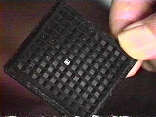
any other power supply. These memory cards (PCMCIA) form a very nice
interface. They are much smaller and more rugged than floppy disks
and ultimately their price will be zero. At the moment they are still
expensive.
(Question about the difference between his software and commercial software.)
OK, let's talk about software. Software is easier to talk about in
a context. But if you look at the programs that are commercially
available, that people are shopping back and forth amongst companies,
my sense is that they are all written in FORTRAN about twenty years ago.
Maybe there has been no software written in the last twenty years.
All that people do is repackage it. Take this package and this package and put them together and have a package that is twice as big and twice as powerful? Well, certainly I can't think of any other way you can get megabytes of software. No one sits down to write megabytes of code. It's probably impossible. You get megabytes by agglomerating kilobytes. You do that one thousand times and you get a megabyte.
It's totally bewildering to me why people are willing to do this. But I talked to someone from DEC who said that their major emphasis in further developments of CAD software was to integrate various software packages into one consistent whole. That one consistent whole could well be megabytes in size even though the individual components are not.
But that is the wrong way to do it. You want to start with a clean piece of paper, decide what you want to do and write some good software to do it. And the first step in doing that is that you have to write your own operating system. And before you can write your own operating system you have to establish an environment that you are going to be working in so that the operating system you can handle everything in that environment. And that is what OK is going to do.
Even in one of these small computers where you have a simple fast processor with a lot of memory, a million words of memory, and problem: a graphics problem where you are going to be designing complex systems such as the chip itself. Now you have got a context in which you can try to optimize something.
The seven input keys are just perfect for that. Seven input keys are no good for word processing but they are just fine for steering cursors around screens and making menu selections. So I start by saying I am going to have seven keys and a menu based driven system. And immediately that establishes some very useful constraints.
First the system is going to be highly modular because all the code is going to be aimed at responding to keystrokes. When I press a button I want to execute a little bit of code that does what that button has directed, moves a cursor on the screen perhaps. The OK system does all that work for me. It interprets my keystrokes. It organizes menus. It lets me edit graphics characters. It does all the supporting work that I need to put pictures on the screen.
And it only needs 1000 instructions to do that . Easy to write 1000 instructions. Easy to invest the effort to optimize those 1000 instructions to make sure they are well done.
The CAD package on top of that is going to be another 4000 - 5000 instructions. Perfectly feasible for one person to write. When all is said and done if I want to add capability to the system it means adding another menu. With seven more button presses available, with seven more button presses worth of code necessary to do something. It does not take large quantities of code, it takes well though quantities of code.
In particular you need to avoid writing code for situations that will never arise in practice. You need to avoid writing code to handle a general problem that you are never going to encounter. For instance the first version of OK was intended to design 40 pin chips. That was the chip I was designing. I had to modify it to design 64 pin chips when that was the chip the chip I was designing. I will probably have to modify it again to handle 84 pins chips when I am that ambitious.
I do not have a piece of software that will handle N pin chips, even where N is between 40 and 84. I have three versions each is specialized. To add the code necessary to change the number of output pads is certainly possible. But I don't need to solve the general problem when I only have to solve these specific cases.
I see a future in which we have not so many general purpose computers and more special purpose computers. Special purpose computers are much easier to program. You don't need to worry about the consequences to your word processor of the changes that you are making to the graphic user interface because their is no word processor.
It's the dinosaurs that insist that computers must be general purpose that are going to go out of business in the next ten or twenty years. Computers will be built into everything but they won't be the same computer. The interfaces won't be the same, they don't need to be the same. A lot more custom silicon.
Being in the custom silicon business I guess that is a natural thing for me to say. And it's certainly not universally accepted in the industry. A lot of people keep thinking that if it can't run 'C' that it can't be interesting. In one hundred years there won't be anything that runs 'C' so it doesn't matter.
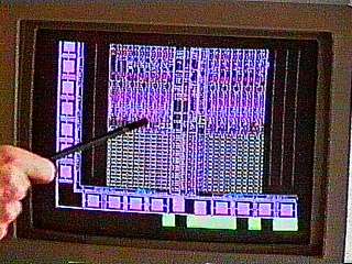
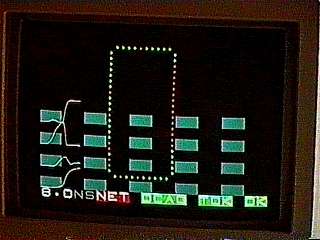
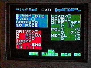
(Chuck switches to a demo of OKAD and tour of the F21 chip layout.)
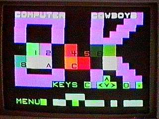
There is the OK screen. If I hit the CAD button we switch to the
CAD screen.
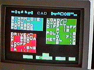
If I hit the rectangle button we get the rectangle
display where we can see the whole chip if I zoom out a bit. Actually
it possible to zoom and see the whole chip. You can zoom way
out and see
The interesting thing is to zoom in to where you can see some of
the geometry of the chip.
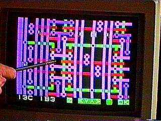
(Why don't you zoom back a little and show what each of the different layers are?)
OK. Here is a region of the stack.
There is the second metal, ground off.
There is the diffusion and wells.
There is just one region of diffusion.
There is just the other region, P vs N diffusion.
There is just the wells.
There are all the diffusions together with the wells.
There are just the substrate contacts.
There's just the poly.
There's just the metal.
There's the metal plus contact.
There is just second metal.
There is second metal plus contact.
There is all of them together.
There is second metal removed.
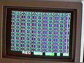
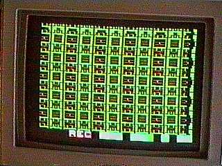
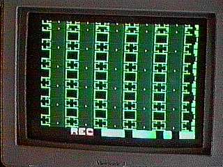
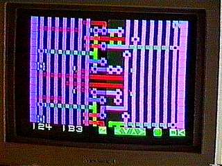
You can see the, oh, I accidentally hit the rectangle button. The reason the rectangle but is in red is to warn you that if you hit that button the computer is going to be busy for ten seconds recomputing, reextracting all the geometry from the tile representation. It takes that long to compute 80,000 rectangles which is fair to midland fast.
Let me zoom in again here. Now you can see a couple of interesting things.
Transistors are regions where poly crosses diffusion, where red crosses
green.
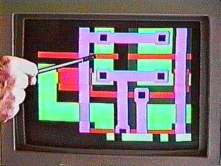
So this is a transistor and this is a transistor.
This is an N transistor because its background is black.
This is a P transistor because its background is greenish, it is
in the N well.
The transistor is controlling the flow of current from here to here. So this is a transmission gate. This pair of transistors constitutes a transmission gate where signals can go from zero to five volts or from five volts to zero with equal facility. Basically these transistors control a switch between these two metal lines.
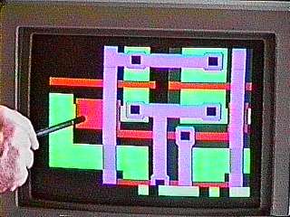
Now this is a very large transistor, physically large. But its geometry is such that
it only conducts 1/10 the current that this one does. And likewise this
transistor conducts only 1/10 the current of that one.
Here is another pair of transistors down here that constitutes an inverted.
These two inverters, cross coupled inverters, constitute a latch. And this
is one of the transmission gates enabling input into the latch.
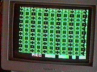
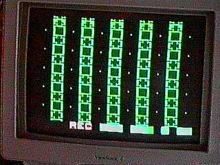
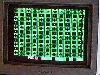
So what we have on the screen now constitutes about one bit of memory.
Control lines tend to be silver and the busses tend to be blue. And this whole thing constitutes about one bit of memory. If we zoom out a little bit now you are seeing two or four bits of memory, and now you see about six bits of memory, and now about a thousand bits of memory.
This entire structure here, this region is the data stack. It is
16 registers by 20 bits so that is 320 bits of memory right here.
Here's the ALU of the processor. If we go up a bit we find the
return stack here. The instruction registers are in this region.
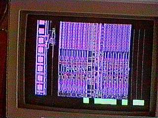
Registers are organized horizontally. So bits zero though twenty are
stretched across the screen horizontally. In the center you find big
transistors to drive the control lines. Here is some random logic
instruction decode to select the control lines.
Here is the return stack. Here is the memory processor. It is spread
out a bit, I have
been moving things around a bit.
Here is the
video coprocessor. Lots of empty space I can use to increase the depth
of the stacks or whatever. This is the analog coprocessor.
This is the network coprocessor.
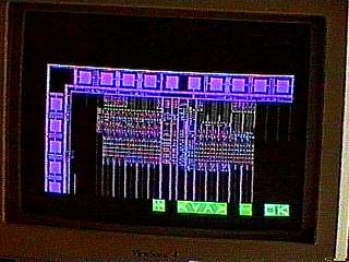
Here is the parallel port which
is attached to the pads and so on.
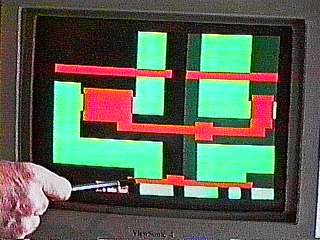
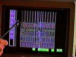
Oh we haven't even looked at the tiled representation.
This is the
tiled representation as distinct from the geometric representation that
we looked at before. Your saying the same things except they are not
scaled to the actual geometry required by the fabricator.
They are more or less the right thickness of lines but only approximately.
This is where I work and edit and simulate the design and then later the rectangles are generated to actually proved the output required for fabrication. Here I have the ability to simulate the behavior of the chip.
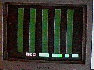
If I hit this button we are now reset to all signals start at zero except
these three pads which represent five volts. We are looking at four traces
at the varying time. Power has ramped up from zero to five volts by now.
You are seeing the 64 pads of the chip change from plus five to ground as
time goes on. So we can monitor 64 signals here and four signals in
great detail here. Each of these squares is 8ns across.
Typically the first interesting event is going to occur about here were we have the first memory access. You see these signals going from ground to five. Now the address lines have been established correctly. This is the SRAM select bit which has gone low. This eight bit data word has been put on the input lines. It represents semicolon so that I will switch from SRAM to DRAM.
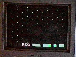
If I stop this process and go back to the tiled layout. We are in a
position to see that the bright red signals have got five volts on them
and dark red signals have got ground on them. So we have established
the signal levels for twenty five hundred signals on the chip.
I can pan though the ... (end of the edited two hour tape #1)
I can show you a few more things.
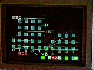
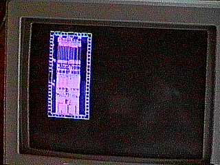
Here are the IV curves of the transistors.
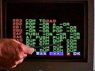
Here is the code I am going to be simulating. This is P21 code...
![]()
UltraTechnology
2512 10th Street
Berkeley, CA 94710