More on Forth Engines
Volume 16, September 1992
Contents
Moore on Forth Engines
. OK
. CAD
. MuP20 Application Notes
Ting's Corner
. the OK-CAD System
. P20A2 Circuit Board for P20 Chip
. eForth System Words
. 386 eForth, a 32 Bit Forth for 80386 Protected Mode Operation
Reprints
. FRP 1600 - 16Bit Real Time Processor, Klaus Schleisiek-Kern
. FRP 1600 Prototype Board for Time Critical Applications
. Forth CMOS RISC Processor FRP 1600
. Writable Instruction Set Computers, Jack J. Woehr
. Ramtron Samples EDRAM
Letters
. Dennis J Perkins
. P.M. Lawrence
. Les O. Archuleta, Kachina DTM Inc.
. Tim Hendlass, Swinburne Institute of Technology
. Wayne Morellini
. Paul Newland, AT&T
. John Amson, Positron Navigation
New Products
. Dr. Julian Noble, Scientific Forth
. Mountain View Press, The Forth Source
. Bradley Software, Forthmacs-386 C Forth
. Orion Instruments, Logic Analyzer, 8800 Emulator
. LMI Forth system, WinForth
. MicroProcessor Engineering Ltd
. Offete Enterprises. 386 eForth
i
Well. Chuck Moore gave the first P20 design to Orbit Semiconductors in mid April and the prototype chips came back in June. I laid out the printed circuit board and collected all the parts and components. We loaded the board and started to test the chips. To our disappointment, the chips did not work. There was no sign of life.
Chuck spent a whole month probing the chips and tried every trick to get the chips to do something to no avail. The greatest fear was that the on-chip oscillator would not oscillate, and consequently nothing would work. But Chuck saw evidence that the oscillator might have worked, because some of the chips drew signifigant current after power was applied, and occasionally he saw intermittent oscillations on some pins at about 50 MHz. Lacking the capability to probe the circuits on chip, it was very difficult to determine exactly what was troubling the chip.
Failing to coerce useful information from his chips, Chuck went back to the design and reexamined every component. He also improved the simulator so that it began to produce results more closely aligned to the silicon data provided by Orbit. He then determined that the most likely cause of failure was that a pair of transistors in the memory timing circuit was accidently inverted. It was unable to generate the proper timing signals to the memory interface. That part of the circuit was not fully simulated because it took to long to simulate the delay loops in the memory timing circuits. To exercise the CPU, he had to shorten the memory delays so that he could see the CPU functioning in a reasonable time frame.
After determining the cause of trouble, and with a higher confidence on the improved simulator, he began relentlessly revising the design. One more bit was added to the architecture, so that the chip was called P21 now. The extra bit is the carry bit in the ALU operations, and is used to select SRAM in the memory coprocessor. The SWAP instruction was sacrificed because it would require and extra latch on the data stack and the control logic would be too complicated. Chuck was musing about how Forth programmers would react to a Forth chip without SWAP. However one can easily access the second item on the stack by >R. He talked to Jeff Fox about it, and Jeff assured him that the P20 eForth could be programmed without SWAP.
The depth of the data stack was increased from 4 to 5. Chuck considered that a depth of 5 is optimum because it allows a very efficient MOVE operation. The control logic was improved as he started to document the logic equations and the timing in the pipeline. The driving circuitry of the I/O pads was also improved. The poly lines were shortened and more connections were shifted to the metal2 layer. By shifting the via off-center, he could pack the metal2 lines closer together and he did use many more metal2 lines to carry the control signals to the transistors.
Late July and early August, he became much more relaxed and was quite satisfied with the improvements he had made. Much more time was devoted to simulation and the results were getting better. At August 19, the P21 design was delivered to Orbit for the second prototype run. We are holding our breath, waiting to see the verdict in 5 weeks.
ii
Thank you all for your continuing intersts in the development of this chip. I have received many letters and phone calls asking me about the progress, and offering encouragement and suggestions of new applications. I just hope that we will get a working prototype soon and proceed on to the production phase.
In the mean time, lots of things are happening in the field of Forth Engines. At the Rochester Forth Conference this June, the Russians were showing their NC4000 clone and the multilayer board hosting the chip. The Germans were also showing an NC4000 clone. Klaus Schleisiek-Kern gave me the literature on his FRP 1600 and the permission to reprint it in this volume. Glen Haydon is still carrying on the WISC development. His plan is to first reduce the 16 bit design to silicon using standard cell technology. Once problem was that the 181 ALU cell does not do what's required, but he had already made an improved cell in its place. The John Hopkins APL group is also continuing on their FRISC chip development.
I have collected man new product announcements at Rochester and include some of them in this volume. I am especially interested in the Forth for 80386. It is becoming a pretty crowded field as well. Forth, Inc., LMI, and Bradleyware all have 386 Forth operating in the 32 bit protected mode. I think we have beaten this chip to death with all these Forth implementations.
Chuck is preparing more documentation on his OK and CAD system, as well as the new developments in the P21 design. I am sure you will find his articles interesting and provoking. As I am privileged to use his CAD system, I put together a report on the OK-CAD system from a user's point of view.
On the eForth front, I am trying to improve the system documentation by first explaining the functions of the high level system words like COLD, QUIT, EVAL, CATCH, THROW, etc. Many of these words are fairly complicated and are not very easy to comprehend, especially to the new Forth users whom the eForth is catering to. Eventually it will evolve into something like the Systems Guide to figForth. I think the documentation on these system words are of interest to you, even if you are not using eForth. During the summer, I ran a short tutorial introducing Forth to new Forth users. The materials are organized in 6 lessons built on a set of 90 Forth words. However, the lessons are too elementary for this audience. If you are interested in using them to teach a beginner's class, you can ask me for the lessons on a floppy disk.
Summer is over. Maybe we all should go back and do some serious work. With the best wishes,
C.H. Ting
San Mateo, California
September, 1992
iii
OK
Chuck Moore, Computer Cowboys
OK has the capabilites of Forth, but is simpler. It does not use disk since computers have large memories. It has no editor or compiler for it composes and displays object code. It has no interpreter but is menu-driven from 7 keys. it has no multi-tasking.
ENVIRONMENT
OK has been evolving for 5 years. It is a sourceless programming system that displays code by decompiling. This eliminates the syntactic difficulties that source code encounters - even in Forth source. It runs on the Novix 16-bit, ShBoom 32-bit and 80386 processors and is destined for my MuP21 processor.
With the elimination of source code, a QWERTY keyboard is no longer required. Rather, a 7-key pad or a 3-key chord pad is a simple, friendly device. Use it to select among 7 enu entries and you have the good features of a pointing device without the complexity. Yes, it is not suitable for word processing.
The 386 version of OK runs under DOS with a VGA display. In a 65KB segment, about 2K is object code, 8K tables, and the rest is free. There are 7 displays of 20 x 15 characters in 16 colors. With them you define your own words, menus and screens.
To start OK type LOAD OK Then type HI (OK is the file name) A screen is displayed which shows which 7 keys are active. Each key executes the function - a Forth word - indicated on the bottom line. Red labels indicate functions that may be dangerous, but the worst that can happen is that you must reload the program.
When you return to DOS you may type SAVE OK to save changes. You may type HI to reenter OK.
MENU
Keys are multiplexed by moving through a menu tree. The most common key function is to select another menu. In effect, the space-multiplexing of a large keyboard is replaced by time-multiplexing a small one.
Implementing a menu is simple. The word MENU saves it return location in a variable 'MENU. When a key is recognized, it is reduced to an integer 1-7 and used to jump indirect through a table at 'MENU. Half a dozen instruction replace the Forth interpreter.
The 0th menu position is use for time-out. If a key is not struck in 5 minutes, that entry is invoked. It may do nothing, jump to a different menu or blank the screen. Actually, menus do not call oneanother, they jump. Thus there are no restrictions on access and no need to return whence you came. And no need to clean-up the return stack. A menu is analogous to a Forth vocabulary.
1
DISPLAY
The whole purpose of OK is to manage a video display. As I get older, I appreciate large characters. Also, I believe the dictum of slidewriters that you limit the information you attempt to present to one image. This leads me to format a screen into some 20x 15 large characters. With VGA, the means 32x32-bit characters, enough resolution for pretty ones. Again, this is not suitable for word processing.
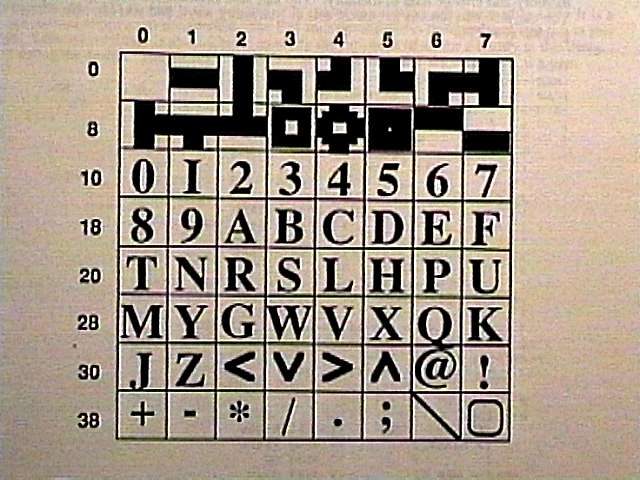
In the spirit of experimentation, I defined a new character set. ASCII derives from the shift QWERTY. Surely there's a better way. I define 48 characters in the order:
0123456789ABCDEF
TNRSLHPUMYGWVXQK
JZxxxx@!+-*/.;xx
This is a combination of hex, English frequency, and Forth opertors. In addition there are 16 graphic symbols. I scroll thru these to compose displays, but I don't do it a lot. If I ever needed to transmit them, I'd convert to ASCII.
Color is important. I like to choose from 16 foreground and background colors for each character. Thus a character requires 4+4+6 bits to display. Round up to 16 bits. There are 3 ultilites included in OK. One selects the 16 colors you want to use, if you get a choice. I like strong primaries.
SCREENS
I'm resurrecting the old Forth term 'screen' as a 20x 15 display. Another utility is an editor for composing such. (The 3rd is a bigbit utility for designing characters).
It's not hard to compose screens. The hardest thing is deciding how you want it to look. You don't do it a lot.
MEMORY
Memory is the most important aspect of a computer. Processing speed (especialy arithmetic) is not nearly as valuable as memory access. A programming system must be able to display memory. OK will display 15 words of memory: address in red and content in green. keys exist to:
2
To this basic display, a programming system adds the ability to name locations. The Forth dictionary becomes a table of names and addresses, ordered by address. The memory display replaces addresses with names whenever possible - in red. Each menu entry is named, as well as application code and variables. Keys exist to:
This editing is done in place on the memory display.
The layout of memory is simply 5 regions:
An application can expand these regions, or can create new ones. The dictionary can include a type code that the memory display uses. For instance, to distinguish hex from decimal data.
DECOMPILER
The decompiler is a major motivation for the system. It can easily be a cross-decompiler, decompiling code for a different processor. It is most useful for Forth processors, with their simple, readable instructions. The 386 is really not suitable.
The decompiler replaces object code with equivalent instruction mnemonics. These come from an mnemonic table. Named routines are identified from the dictionary, as with the memory display. As are the destinations of jumps. With Forth at least, it's convenient to put several instructions on a line. OK displays instructions in green, addresses in red and literals in blue.
Keys are needed to:
Since names are referenced from addresses, they need not be unique. Thus different menus/applications can use the same names in their private context.
3
CAD
Chuck Moore, Computer Cowboys
The chip design is based upon the actual, geometric layout of 5 layers. This is distinct from normal practice where designs are based upon a schematic. CAD does not use or product schematics. Of course, the designer may use them outside the system.
This approach is a matter of personal choice. Silicon compilers, schematic capture and auto-routing are bing well explored. Other alternatives are not. I have found it fun to draw brightly-colored graphic images; and fun to animate them. The Forth computer language lets me undertake ambitious software, and provides the goal of designing an efficeint Forth microprocessor.
As is often the case, available tools influence the design. For example, CAD can properly simulate tranmission gates, which encourages their use. I can see, and look forward to distinctive designs.
4
LAYOUT
A chip is represented as an array of tiles. For example, my MuP21 microprocessor die is 2.4mm square. I format it as a 600x600 array of 4x4um tiles. Each tile uses 4 bytes of memory, so the chip uses 1.5MB.
The present version uses 5 layers to represent well, diffusion, polysilicon, metal-1, and metal-2. Each layer uses 4 bits of the tile to choose one of 16 patterns: blank, horizontal, vertical, corner, contact, etc.
A VGA display provies 640x480 pixels of 16 colors. I format it into a 20x15 array of 32x32 pixel characters and darw the tiling patterns in 8 colors:
Bright green, red and blue label nets at 5 volts, as opposed to ground, as determined by the simulator.
The layers are stacked in their physical order. They may be peeled off to examine detail otherwise they are concealed. Transparent colors are not adequate to look 5 layers deep.
Most of my time is spent working with these tiles. The 7 keys are programmed to provide a variety of actions:
With such a layout tool, it is practical to hand-craft chips. The advantage of manual place and route is that you know what you get. If there is no room for a gate, or if a trace is unfortunately long, you can reconsider the design. The goal is a clear, compact layout and you can continually evalute your progress. Such an approach is most useful for microprocessor and memory layout, and probably innappropriate for random logic.
5
NETWORK
The first step in verifying a layout is to extract the transitsors and the nets to wheich they're connected. The MuP21 is in 1.2um CMOS with 6500 transistors connected to 2500 nets. Each transistor is characterized by a drive (uA) and each net by a load (fF).
To facilitate net indentification, the program first traces the largest nets, power and ground. It starts at the input pad and uses a recursive algorithm to follow the trace through metal-1 and diffusion, branching is required. It marks each tile with a flag:
1. Computing capacitance based on fF/tile for each layer:
6
SIMULATION
Armed with transitor and net tables, the program can simulate the chip. Apply 5 Volts to the power net and observe the consequences. Because all the nets have a capacitive load, there is no DC bias matrix to solve. Simply integrate the differential (difference) equations:
As with any model, you don't include unnecessary detail. Thus, I don't include poly resistance (80 Ohms/tile), but promise that it is negligible. Arithmetic is low-precision integer (16-bit), a version of fuzzy logic.
My current transistor model is:
The time step wants to be large for speed, but is limited by the smallest capacitance. In order to insure that the voltage change on an internal node is about 1 volt, it must be 32ps. It can be variable, since signals mostly change during clock ticks, but that doesn't help much. Simulation is slow on 386. The purpose of the MuP21 I've designed is to speed that up ten times.
While a simulation runs, 4 scope traces can be displayed. Merely point to a metal portion of 4 nets to select the signals. Rise times, phasing, amplitudes and glitches are easily determined. Four seems the limit of my memory as to which trace is which signal.
Having run a simulation, the final signals levels (above or below 2.5 Volts) are indicated ont he tile display. Now there are 2500 signals at the same time. In particular you can check the logic and sense of control signals. I persist in changing NAND and NOR gates and miscounting the number of inverters.
A future enhancement will record the time of transition (thru 2.5 Volts) for each signal. This will allow easy verification of phasing and control signals relative to the clock. It is also an example of continual improvements you can make if you write the software.
7
TAPE-OUT
The geometry so far has been purely schematic. The 4um tiles determine the model for load and drives. The basic layout is scalable.
The trace widths for each layer are specified by the design rules. Tile size must be chosen so that separations are adequate. This is inevitably the separtion between the adjacent contact. With 4um tiles, this is met except for metal-2, where traces may not be adjacent to vias.
The simplest GDS II (or CIF) tape is composed of rectangles. I scan each layer horizontally (vertically for metal-1) and compose the largest rectangles for each trace. A second scan extracts contacts/vias. In the case of vertical traces, it's necessary to mark visited tiles to avoid revisiting them.
The MuP21 layout requires 65,000 rectangles. My format records 2 bytes for each of 4 coordinates - x and y for lower-left and upper-right corners - or 8 bytes/rectangle. This is then expanded to 20-30 bytes in the cleverly-designed standard formats, and then ZIPed to fit on a floppy.
TO view this actual geometry, as well as verify the rectangle decomposition, keys are defined to:
8
MUP20 APPLICATION NOTES
A principle design goal is to minimize system - hardare + software - complexity. These notes explain some resulting tradeoffs. ...
The OK-CAD System
OK is the new Forth-like system Chuck Moore created as his programming environment. It uses lots of ideas from Forth, but is does not use the text based interpreter/compiler user interface. Instead, the user controls the system with a 7 key keyboard and the system puts its responses on a 24x16 tiled color montior. It resembles a video game more than a programmable computer.
The main purpose of the OK system is to support the CAD system, which Chuck uses to design and simulate his new Forth chips. Since the layout, design, modification, and simulation of circuits on silicon are fundamentally graphical activities, OK is perfectly suited with its unique user interface.
System Organization
OK is implemented on a 386 DOS compatible computer. It requires at least 4MB of memory, a VGA card and monitor, and a 40MB hard disk. To avoid dealing with the complexity of the DOS system, the OK system is first loaded into memory above the DOS 1MB area. The CAD data is loaded above the 2MB regoin. Then all the system interrupts are disabled, the 386 protected mode is activated, and OK is started.
Existing functions in OK can be accessed using the 7 keys on a keyboard, through a series of menus displayed at the lower right corner of the screen. The user can inspect memoyr and modify memory contents. By modifying memory, one can add new functions and change existing functions. Jumping into the CAD system, the user can inspect the current CAD design in the tile format or in rectangles. He can change the design by changing the tiles, which form transistors, metal and poly conductor traces, vias, and contacts.
OK does everything in the RAM memory, and it does not need any DOS service while it is running. After the work in OK is done, one can return to DOS and save the modifications in either OK or the CAD design by saving the changed images to DOS files. There are several important advantages in this system configuration: the complexity of DOS services is isolated and eliminated from the OK system proper; the large addressing space and the ALU power of the 386 CPU are fully utilized; and the user interface to programming the CPU design is greatly simplifed.
The DOS interface
The most important feature the DOS system provides is a portable file system which allows us to save data and code in large files on hard disk and transport these files to other computers on floppy disks. The OK-CAD system makes use of this service with a set of small programs:
14
A small batch file HI.BAT is used to initialize OK through DEBUG. A DUMP.BAT file is used to automate backing up the system onto a 1.2MB floppy disk. it uses PKZIP to compress the P21. data file. A typical OK-CAD session involves the following DOS commands:
After doing your work in OK, back-track to DOS using the Del key. If you changed things in OK, save the changes with SAVE. If you changed things in CAD, save the changes with WRITE. Then backup the system with DUMP:
In the protected mode, 386 allows us up to 4GB of memory. For the OK and the CAD system only 4MB are required. The memory utilization is shown in the following memory map:
0000:0000__110000____DOS system
xxxx:0100___10000_____LOAD,SAVE,READ,WRITE
xxxx:0150______38_____GDTR descriptors
000A:0000___10000____VGA display
0010:0100___10000____OK code and data
0011:0100___10000____CAD code and data
0012:0100__100000____Chip layout
0020:0000____________Net and transistor lists
0011:FFFC____1000____Stack
15
_0____Reserved____0000:0000
_8____Code_______0011:0000 4GB linear space
10____Data________0011:0000 4GB linear space
18____VGA_______000A:0000 64KB limit
20____Dump_Data__0000:0000 for SAVE and WRITE
28____INT_Vector__xxxx:0280 Return to DOS
30____Data________xxxx:0300 Return to DOS
The Character Set
The OK character set is another of Chuck Moore's inventions. It is designed as part of the user interface of OK, and has the building blocks to the CAD circuit layout system. it is quite unconventional, as everything else Chuck did. However, it is well suited for the environment, and it service well its designed purposes.
The character set consists of 16 graphic patterns for chip design, 16 hexadecimal digits from 0 to F, 18 alphabets, and 14 miscelaneous characters and symbols. The symbols include up, down, left and right arrows, which are important in matching the cursor movement keys on the 7 key key keyboard. These characters are shown in Figure. 2.
You will notice that the alphabets O and I are not included, because you can use 0 and 1 instead. The alphabets A-F are in their normal order, following the numerals. The other alphabets are arranged in the frequency of usage order. The charactrs @, !, +, -, *,/,,, ;, and \ are included they are familiar Forth words and have generally accepted connotations. The last symbol is a rectangle with rounded corners, and it is called 'ring'. It is generally used in the OK and CAD system to highlight a character or tile like a cursor for some editing functions.
The 16 graphic symbols are used to express IC circuitry, like n and p diffusions, traces of polysilocon and metal, vias and contacts. Chuck uses them to construct transistors, transmission gates, and the connecting traces among them to form sophisticated circuits in a high speed Forth microprocessor. It is amazing that the highly complex VLSI design can be expressses in such a simple set of primitive components.
OK comes with a symbol editor which allows you to change the patterns of these symbols to suit your own applications. Therefore, OK can be customized for applications other than chip design and layout. OK is a simple 2K GUI. Each symbol is designed in a 32x32 matrix, and you can edit any dot in the matrix. (Please be reminded that I-Ching, The Book of Change, handed down from ancient China, was based on 64 categogies in analyzing everything that can be analyzed).
16
The Character Set
The Menu Tree
Chuck has been experimenting with this 7 key interface for almost 10 years and this implementation seems to be the most useful and productive. Here on a regular 101 key keyboard, he uses only 7 keys on the lower right corner of the keyboard: the right CTRL key next to the space bar, the four cursor arrow keys, the INS key, and the DEL key. These 7 keys are grouped together and can be acessed by four fingers on your right hand. The index finger rests on the left arrow key, the middle finger handles the up and down arrow keys, the ring finger rests on the right arrow. The little finger moves over the INS and DEL keys and the thumb is used to hit the CTRL key. The thumb action is a little bit awkward, but the CTRL key is not used very often and its function is sometimes destructive.
The 7 keys allow you to select one function among 7, from a menu displayed on the lower right corner of the screen. The labels in the menu mostly are farily intuitive and you can follow them very easily. The functions with destructive effects are assigned brightly red labels to serve as warnings. There is an eight function in every menu. It is activated after 5 minutes of inaction. This hidden function usually turns off the monitor or retrace to the previous menu if functions in the current menu could cause data to be destroyed when a key was pressed by accident.
17
The following table shows the menu tree in OK. You can explore the system by examining the memory and changing data in memory. You can also examine the memory using the decompiler. You also edit screens to present text in interesting ways, and you can also change the text and graphic symbols.
|DOS     |OK      |
|MEM     |SQ      |OK
|CAD     |        |> move cursor
|SYM-|   |        |^ change data
|    |   |        |v change data
|    |   |        |< move cursor
|    |   |CODE-|  |NAME-|
     |         |        |
     |         |        |--|
     |         |           |
     |         |           |> move cursor
     |         |           |^ change label
     |         |           |v change label
     |         |           |< move cursor
     |         |           |OK
     |         |--|OK
     |            |
     |            |> decompile up
     |            |
     |            |
     |            |< decompile down
     |            |
     |
     |--|OK       |OK      |OK
        |EDIT-----|TOG     |TOG high-low
        |> next   |        |> drag right
        |         |        |^ drag up
        |         |        |v drag down
        |< prev   |        |< drag left
        |         |DRAG----|
18
The chip design CAD system is the one and only major application programmed in OK. It is a very substantial application nonetheless. The P21 microprocesor is designed and laid out in this system. A circuit simulator is also included to verify the functions of all the circuitry in this design, and to debug the design. The menus to access all the design functions are connected as a tree:
|DOS     |OK      |OK      |OK      |= ------|OK
|MEM     |VIEW----|SQ------|SQ------|OK      |# change symbol
|CAD-----|        |> pan   |> move  |C       |> drag right
|SYM     |        |^ pan   |^ move  |^ cell  |^ drag up
|        |        |v pan   |v move  |v cell  |v drag down
|        |        |< pan   |< move  |< cell  |< drag left
|        |SIM-|   |Z layer |Z layer |ROI     |
              |                     \
              |---|OK               |C-------|OK
              |SQ highlight         |        |
              |REC rectangles       |        |3 set trace 3
              |C continue           |        |2 set trace 2
              |I input              |        |1 set trace 1
              |< reset              |        |0 set trace 0
              |NET netlist          |        |C compute capacitance
              \                     \
              |          |OK        |ROI-----|OK      |OK
              |          |zoom up            |# copy--|S set lower left
              |REC-------|> pan              |> size  |> rot clockwise
                         |^ pan              |^ size  |^ flip on y
                         |v pan              |v size  |
                         |< pan              |< size  |< mirror on x
                         |zoom down          |PRY-|   |DUP Duplicate
                                                  |
                                                  |---|OK
                                                      |
                                                      |> add column
                                                      |^ add row
                                                      |v add row
                                                      |< delete column
                                                      |
Interface to the Real World
After the chip layout is done and the simulation is satifactory, the design will have to be converted to a form that can be read by a silicon foundry to produce chips. While in the CAD system, one has to select the REC option under SIMulator. REC converts th tiles in all layers into rectangles which are plotted on the screen in vivid color. The rectangles are stored in high memory. After exiting OK and back to DOS, the rectangles can be saved to a tape file by the command:
19
![]()
Ultra Technology
2512 10th Street
Berkeley, CA 94710